
Official Assignment Description: 'make the FabISP in-circuit programmer'
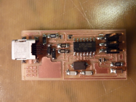
The purpose of this week's project is to fabricate a pre-designed printed circuit board (PCB) with surface mounted device (SMD) components that is capable of programming other electronics devices.
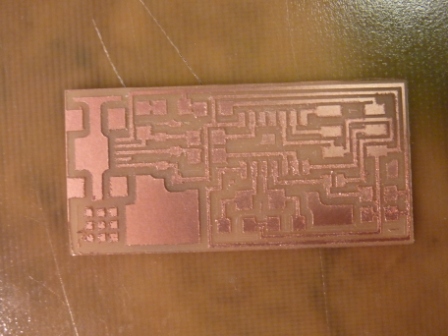
Step 1: Download the two .png files from the MAS website. The machine 'eats chocolate,' so the areas you want milled should be black.
hello.ISP.44.traces.png , hello.ISP.44.interior.png
Step 2: Use Fab Modules to make path and rml files for each .png. Remember to use settings for 1/64" bit for traces and 1/32" bit for border.
Step 3: Use Modela to mill out traces and border separately. Don't forget to change bits in between! Remove burs and check to make sure all traces
look correct.
Step 4: Solder all components. Try to anticipate how / where you will hold the soldering iron and install SMD's in order of ease of access. General
rule is inside outwards. Double check conductivity and resistances with multimeter whenever possible. As PCB tends to slide around during soldering,
I found securing it to the table with a single piece of double-sided tape made things easier.
Step 5: Make insulation displacement connector (IDC) for programming via in-circuit progrogrammer (ICP) connector.
Step 6: Program firmware onto microcontroller.
Step 7: Desolder SJ1 and SJ2.